
This article was originally published on All About Circuits by Stanley Huang from Silicon Motion.
Contact UsAI will push the limits of PCs and smartphones. In turn, demands on storage controller chips will be intense. Learn how chip architectures and firmware schemes must be optimized for these AI workloads.
AI is coming to the edge. In 2025, almost half of new personal computers will execute AI models—including generative AI—locally, according to Gartner. IDC estimates GenAI smartphone shipments will grow at a compound annual growth rate of 78.4% from 2023 to 2028.
This sweeping change will bring exciting new abilities to users of edge-computing devices untethered from cloud data centers. However, the substantial computing loads and enormous parameter files—containing billions of parameters—will put new demands on edge hardware. Computing hardware, interconnect, memory, and storage will all face challenges.
Four Pillars of Storage in the AI Realm
To address the needs of edge AI, storage must deliver optimal performance in four areas: capacity, power efficiency, data efficiency, and security (Figure 1).

Capacity is necessary to accommodate the massive data from GenAI, multiple AI models, or applications such as image generators and other content tools. For example, Phi-3, a very compact small language model by Microsoft, has 3.8 billion parameters and requires around 7 to 15 Gigabytes of storage for just one model. Storage needs will surpass a Terabyte in a system supporting several AI-powered apps.
Power efficiency may be less obvious but just as necessary. PCs and mobile devices must meet tight battery size restrictions and demands for extended operating hours. Storage is an issue here: it can consume 10 percent of the power in a laptop and nearly 5 percent in a smartphone.
Data efficiency is another critical area. How the storage system uses the physical space in the NAND flash chips can influence access latency, overall performance, and flash endurance. All three of these factors would affect the user's experience.
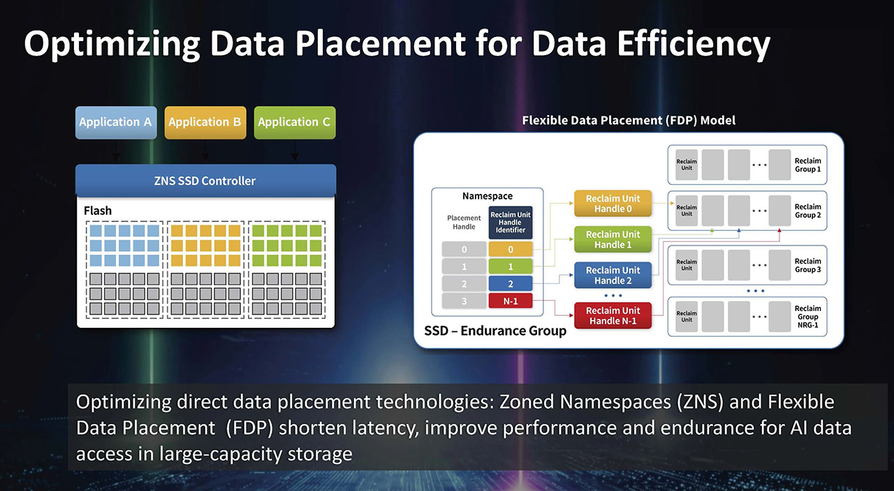
Data efficiency also contributes to power efficiency. But having the data in the right place isn't just a matter of power efficiency. Two NVMe technologies, zoned namespaces (ZNS) and flexible data placement (FDP), optimize data placement for AI apps (Figure 2).
Robust data security will also be mandatory. Parameters necessary for executing the AI models represent months or years of experience and training runs for app developers. The developers will insist that the parameter files be protected. Increasing the use of local AI will encourage users to keep their most personal data locally rather than entrusting it to a cloud.
The storage controller's design heavily influences all four of these areas. A new generation of storage controllers is ready and optimized for the needs of edge AI. At the edge, many form factors require different controller design approaches. We can illustrate this by examining two cases: an AI-ready PC and an AI-enabled smartphone. The two platforms have similar needs but at different scales and constraints.
Storage Performance and the AI PC
An AI-ready PC must have the raw storage performance and capacity to please users of even huge AI models and be able to multitask. Silicon Motion has designed the SM2508 controller for this application. With four PCIeGen5 lanes to move data to the host and eight NAND channels, the controller can reach sequential read rates of 14.5 Gbytes/s. Equally important in a multi-tasking environment where the controller will see a random mix of IO operations, the chip achieves 2.5 million random IOPS.
The controller can manage up to 8 Terabytes of NAND flash to support the capacity needs of the AI workloads. But this figure raises another critical point about capacity. System designers will use the latest quad-level-cell (QLC) 3D NAND flash chips to achieve these huge memory densities. These chips exhibit unique error patterns that require particularly sophisticated—and vendor-specific—error-correction algorithms.
Silicon Motion has developed a machine-learning ECC algorithm that adapts to the error patterns of the storage system's NAND devices as the chips age. This algorithm reduces latency and extends the storage system's endurance. Silicon Motion's history of working with every significant NAND flash vendor means that such features do not lock a system developer into a specific NAND vendor.
The second pillar is power efficiency, which begins with process technology. Silicon Motion chose TSMC 6 nm for the SM2508, organized functional blocks within the chip, and designed-in extensive power management features. As a result, the SM2508 uses only half the power of an equivalent 12 nm controller.
Data Management is Key
Excellent data management can also improve latency, performance, and endurance. Much of a storage system's energy consumption is determined by how efficiently the controller places and moves data within the NAND chips. Leveraging decades of flash-management experience and a detailed understanding of individual NAND chip characteristics, the SM2508 can improve power efficiency by up to 70 percent compared to competitive controllers.
The fourth pillar is security. A secure storage system must start with a secure controller. The chip must itself be tamper-resistant. It must use a secure boot process to lay the foundation for secure authentication, which is necessary to protect its firmware from tampering. The SM2508 meets these requirements.
The controller must also protect the data under its control. The SM2508 complies with Opal full-system security. It supports hardware-based AES 128/256 and SHA 256/384 encryption, which fully protects the data within the storage system without significantly impacting performance.
On-Device AI Smartphones
The needs of the AI smartphone user are essentially the same as those of the PC user: capacity, power efficiency, data efficiency, and security. However, a smartphone's constrained size, weight, and expected battery life demand much lower power consumption and limit the storage system's capacity. For this environment, Silicon Motion has recently introduced the SM2756 controller.
Rather than the performance-tuned NVMe platform, the SM2756 uses the mobile-optimized Universal Flash Storage (UFS) 4 specification. This specification version gives the storage system significant performance advantages over UFS 3.1. The SM2756 takes advantage of this potential by providing a 2-lane HS-Gear-5 interface, employing MPHY 5.0 technology, and reaching sequential read rates of up to 4.3 Gbytes/s. That translates into loading a 3-billion-parameter AI model on a smartphone in under half a second.
To meet the capacity needs of the AI smartphone, the SM2756 supports tri-level and QLC 3D flash devices. It can manage up to 2 Terabytes of storage. Using TSMC 6 nm silicon and aggressive dynamic power management again aids power efficiency. The controller will achieve nearly 60 percent power savings when loading a large parameter file, compared to the power consumption of a similar UFS 3 controller.
As in the SM2508, the SM2756 uses extensive firmware algorithms to optimize data efficiency. Although this is done somewhat differently under UFS 4 than under NVMe, the impact on latency, actual transfer rates, and endurance is similarly substantial.

The SM2756 uses an anti-hacker algorithm code to address security issues. This code prevents hackers from intervening during boot-up, ensuring data integrity and security on mobile devices.
New Demands on Storage Controller Performance
AI applications executing locally on the edge will push PC and smartphone platforms to their performance, capacity, and power limits. Some of this burden will fall upon storage systems. The storage subsystem's performance, capacity, power efficiency, and data efficiency can all visibly affect users' experience with their devices.
Meeting the storage subsystem requirements demands a lot of the storage controller chip. The chip architecture, hardware implementation, and firmware must be optimized for these AI workloads. That requires a detailed understanding of NAND flash concepts and the operational details of individual flash chip families gained by decades of close working relationships with the flash vendors. It is a project that a system developer would want to undertake with others.
Further, the independence of the controller vendor is critical. In today's environment of highly dynamic global semiconductor markets and uncertain supply chains, to be locked into a single flash vendor by the limitations of the storage controller could be a very costly mistake.
Silicon Motion, with its decades of close relationships with all significant NAND flash vendors, its deep understanding of managing data within a storage array, and its explicit recognition of the importance of data security, has brought these strengths to a new generation of controllers for edge AI. We stand ready to support your system design.
Contact Us